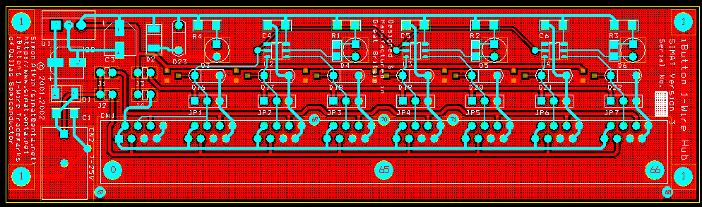
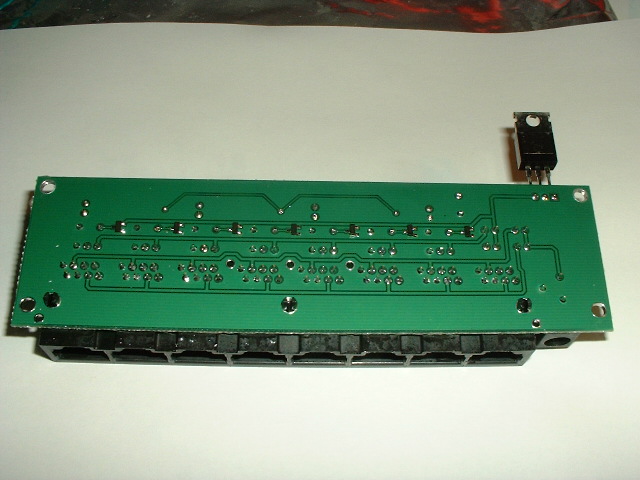
1-Wire Hub Version 3
A year and a half on and it's finally time for another run of 1-wire hub boards. After a year and a half of using OrCad I noticed that the old board design could do with a clean up, so I've re-done the entire layout and added some extra features.
I've added BAT54S's on each 1-wire data line to stop it from going above +5v or below 0v, pads for a transient voltage suppressor on each 1-wire data line to help protect against line transients such as lightning, although some people have reported problems when using TVS's with 1-wire, I'm using a P6KE7.5A from Fairchild Semi and I haven't had problems yet, you don't have to use a TVS you could use a GDT or an MOV or just an ordinary Zener diode.
I've also added reverse polarity / reverse EMF protection to the +5v power lines as well as a TVS for overvoltage / transient protection. The power connector has been upgraded from a 1.3mm to the more common 2.1mm power connection, two parts, the DS2401 CSP and the 33uF capacitor straight after the power connection have been removed as I felt these weren't necessary. The re-routing of the PCB has also produced a much better track layout, that I was happy with, apart from that everything else is still the same.

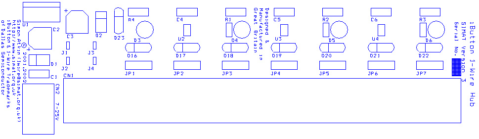

Power Settings:
J1 Connect Unregulated +V to Pin 6 of all RJ45 sockets
J2 Connect Unregulated +V to Pin 3 of all RJ45 sockets
J3 Connect Regulated +5v to Pin 1 of JP1-JP7 headers
J4 Connect Regulated +5v to Pin 1&2 of all RJ45 sockets
Additional Device Headers (JP1-7)
Pin 1 = Regulated +5v (controlled by J3)
Pin 2 = 1-Wire DATA
Pin 3 = GND
JP1 Input connection (bus)
JP2 Main 1-Wire output of U2 (port A)
JP3 Aux 1-Wire output of U2 (port A)
JP4 Main 1-Wire output of U3 (port B)
JP5 Aux 1-Wire output of U3 (port B)
JP6 Main 1-Wire output of U4 (port C)
JP7 Aux 1-Wire output of U4 (port C)